- Главная
- Разное
- Бизнес и предпринимательство
- Образование
- Развлечения
- Государство
- Спорт
- Графика
- Культурология
- Еда и кулинария
- Лингвистика
- Религиоведение
- Черчение
- Физкультура
- ИЗО
- Психология
- Социология
- Английский язык
- Астрономия
- Алгебра
- Биология
- География
- Геометрия
- Детские презентации
- Информатика
- История
- Литература
- Маркетинг
- Математика
- Медицина
- Менеджмент
- Музыка
- МХК
- Немецкий язык
- ОБЖ
- Обществознание
- Окружающий мир
- Педагогика
- Русский язык
- Технология
- Физика
- Философия
- Химия
- Шаблоны, картинки для презентаций
- Экология
- Экономика
- Юриспруденция
Что такое findslide.org?
FindSlide.org - это сайт презентаций, докладов, шаблонов в формате PowerPoint.
Обратная связь
Email: Нажмите что бы посмотреть
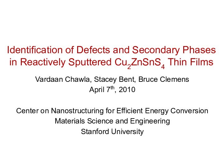
Презентация на тему Identification of Defects and Secondary Phases in Reactively Sputtered Cu2 ZnSnS4 Thin Films
Содержание
- 2. OutlineMotivationProblems with characterization of thin filmsExperimental approachResultsX-ray diffractionRaman SpectroscopyTransmission Electron MicroscopyScanning Auger MicroscopySummary & Acknowledgements
- 3. Motivation – Phase EquilibriumCZTS is a line
- 4. Motivation – Crystal StructureCrystal structures of secondary
- 5. Experimental ApproachSubstrateCuZnSnIntroduce H2S into chamber during sputter
- 6. Characterization - XRDVarying Zn/(Cu+Sn) RatioZn/(Cu+Sn) ratio is
- 7. Characterization - XRDVarying Cu/(Zn+Sn) RatioCu/(Zn+Sn) ratio is
- 8. Characterization – RamanVarying Zn/(Cu+Sn) RatioRaman spectra show
- 9. Device FabricationGlass Substrate3000 µmMolybdenum Layer1 µm1.75 µmCdS
- 10. Device CharacterizationI-V MeasurementEQE MeasurementFirst CZTS devices grown
- 11. Characterization - TEM500nmDetrimental secondary phase interspersed in
- 12. Characterization - AugerRaster beam over sputtered surface
- 13. Characterization - CdZnSCd penetration into ZnS lowers
- 14. Characterization - AugerSnCdOverlay Sn and Cd signalCd
- 15. SummaryCZTS thin films were grown using Reactive
- 16. AcknowledgementsUS Department of Energy, Office of Basic
- 17. Скачать презентацию
- 18. Похожие презентации


Слайд 2
Outline
Motivation
Problems with characterization of thin films
Experimental approach
Results
X-ray diffraction
Raman
Spectroscopy
Слайд 3
Motivation – Phase Equilibrium
CZTS is a line compound
between Cu2SnS3 and ZnS
Theoretically even a 2-3% compositional variation
could lead to phase separationTernary Phase Diagram
Binary Phase Diagram
Olekseyuk, I.D. "Phase Equilibria in the Cu2S-ZnS-SnS2 System." Journal of Alloys and Compounds. 368. (2004): 135-143. Print.
CZTS
Слайд 4
Motivation – Crystal Structure
Crystal structures of secondary phases
similar to CZTS
All primary peaks overlap and hard to
separateLow intensity peaks cannot be seen easily in thin films
Theoretical XRD Patterns of CZTS, Cu2SnS3, and ZnS
Слайд 5
Experimental Approach
Substrate
Cu
Zn
Sn
Introduce H2S into chamber during sputter deposition
Sulfur
is incorporated into the film in one step (no
anneal)Expect to see higher densities and improved film quality
Reactive Sputtering
Слайд 6
Characterization - XRD
Varying Zn/(Cu+Sn) Ratio
Zn/(Cu+Sn) ratio is varied
while holding Cu/Sn ratio constant
Impossible to determine difference between
CZTS, CTS, and ZnS from XRD pattern(101)
(200)
(220)
(312)
(112)
Olekseyuk, I.D. "Phase Equilibria in the Cu2S-ZnS-SnS2 System." Journal of Alloys and Compounds. 368. (2004): 135-143. Print.
Слайд 7
Characterization - XRD
Varying Cu/(Zn+Sn) Ratio
Cu/(Zn+Sn) ratio is varied
while holding Zn/Sn ratio constant
Need to get very far
off 2:1:1 stoichiometry before any CuxS phases can be seenCuxS can be removed with KCN etch
(101)
(200)
(220)
(312)
(112)
Olekseyuk, I.D. "Phase Equilibria in the Cu2S-ZnS-SnS2 System." Journal of Alloys and Compounds. 368. (2004): 135-143. Print.
Слайд 8
Characterization – Raman
Varying Zn/(Cu+Sn) Ratio
Raman spectra show only
minor changes even though composition is varied dramatically
No evidence
of the CuxS phase shown by other groups at growth temperatures higher than 500CVarying Cu/(Zn+Sn) Ratio
Слайд 9
Device Fabrication
Glass Substrate
3000 µm
Molybdenum Layer
1 µm
1.75 µm
CdS (n-type)
55
nm
ZnO:Al (n-type)
340 nm
Aluminum Grid
CZTS Absorber (p-type)
CZTS Device Stack
Zn-rich films
incorporated into standard CIGS device stack for testingZnO
85 nm
ZnO
ZnO:Al
CdS
CZTS
Mo
SEM Image
Слайд 10
Device Characterization
I-V Measurement
EQE Measurement
First CZTS devices grown by
a reactive sputtering process
Efficiency = 1.35%
Degraded EQE clearly points
to undetected defects in the absorber
Слайд 11
Characterization - TEM
500nm
Detrimental secondary phase interspersed in CZTS
matrix
Stacking faults in the secondary phase point to a
transition between cubic and hexagonal crystal structures
Слайд 12
Characterization - Auger
Raster beam over sputtered surface of
sample and scan for Cu, Zn, Sn
Overlay Cu, Zn,
Sn signalComposition variation points to CZTS / ZnS (Zn-rich)
2 um
Cu
Zn
Sn
CZTS
ZnS
Слайд 13
Characterization - CdZnS
Cd penetration into ZnS lowers the
cubic-hexagonal transition temperature
Stacking faults in TEM images are created
during CBD of CdS layerCdS – ZnS Phase Diagram
(101)
H-ZnS
(220)
(312)
(112)
XRD before and after CBD
C
C + H
H
Chen et al.“Solid State Phase Equilibria in the ZnS-CdS System." Materials Research Bulletin. 23. (1988): 1667-1673. Print.
Слайд 14
Characterization - Auger
Sn
Cd
Overlay Sn and Cd signal
Cd ion
exchanges with Zn during bath deposition and penetrates the
ZnS phaseCZTS
CdZnS
2 um
Слайд 15
Summary
CZTS thin films were grown using Reactive Sputtering
Films
were characterized using X-ray Diffraction and Raman Spectroscopy
Full devices
have been grown and tested but are limited due to secondary phases in the filmsTransmission Electron Microscopy and Scanning Auger Microscopy can be used to identify these secondary phases
Слайд 16
Acknowledgements
US Department of Energy, Office of Basic Energy
Sciences as part of an Energy Frontier Research Center
http://www.er.doe.gov/bes/EFRC/index.html
Applied
Quantum TechnologiesLocal thin film solar startup
http://www.aqtsolar.com
